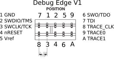
Debug edge is an open standard for exposing debug signals such as SWD and JTAG on the edge of a 1.6mm printed circuit board (PCB).
It uses low cost board-to-board connectors to that no part is needed on the target PCB. This minimizes cost for everyone but ensures easy debug access when desired.